Transformerless power supply. Principle of operation
I needed a power supply for a homemade mini-drill made from a 17-volt motor. I reviewed many circuits of various power supplies, but they all used a transformer, which I don’t have, and I’m somehow reluctant to buy. Then I decided to do something simpler and collect power for this voltage - 17 Volts. The circuit is quite simple, such a ready-made power supply needs to be supplied with 220 volts of alternating voltage, in short, power the circuit from an outlet, and at the output we get 17 volts of direct voltage. Typically, power sources of this type are used in all sorts of small household things, for example, in a flashlight with a battery, as a charger, where a small current is needed, up to 150 mA, or in electric shavers.So, details for the diagram. This is what the high voltage metal film capacitors look like (the red ones), and to the left of them is a 100 uF electrolytic capacitor.
![]()
Instead of a microcircuit 78l08
You can use voltage stabilizers such as KR1157EN5A
(78l08) or KR1157EN5A
(7905).
![]()
If there is no rectifier diode 1N4007
, then it can be replaced by 1N5399
or 1N5408
, which are designed for higher current. The gray circle on the diode represents its cathode.
![]()
Resistor R1 was set to 5W, and R2 - to 2W, for insurance, although both could be used at 0.5 W.
![]()
Zener diode BZV85C24
(1N4749), designed for a power of 1.5 W, and for a voltage of up to 24 volts, it can be replaced with a domestic one 2С524А
.
![]()
This transformerless power supply was assembled without adjusting the output voltage, but if you want to organize such a function, then simply connect a variable resistor of approximately 1 kOhm to pin 2 of the 78L08 microcircuit, and its second pin to the minus of the circuit.
![]()
Of course, there is a board for the transformerless power supply circuit, it’s in Lay format, you can download it. I think you understand that diodes without markings are 1n4007
.
![]()
The finished structure must be placed in a plastic case, because the circuit connected to the network is under a voltage of 220 volts and under no circumstances should you touch it!
![]()
In these photos you can see the voltage at the input, that is, the voltage in the outlet, and how many volts we get at the output of the power supply.
Video of the operation of a transformerless power supply circuit
The big advantage of this scheme
The dimensions of the finished device can be considered very modest, because due to the absence of a transformer this power supply can be made small, and the cost of parts for the circuit is relatively inexpensive. Disadvantage of the scheme we can assume that there is a danger of accidentally touching a working source and receiving an electric shock. Author of the article - egoruch72.
Discuss the article TRANSFORMERLESS POWER SUPPLY OF CIRCUITS
So, let's look at the sequence of calculating the transformerless power supply discussed in the previous article. The described method does not claim to be the ultimate truth and may differ from other sources. Additional information on this scheme can be found on foreign resources by googling the query “capacitor power supply” on the Internet.
rice. 1
1. Calculate the load current
The first thing we should start from when calculating a transformerless power source is the load current. In Figure 1 it is designated as Iam, and resistor R3 acts as a load. Let's replace this resistor with a small circuit with a microcontroller and determine the current it consumes.

rice. 2
You can do this in two ways:
- by calculation, summing up the approximate consumption of all components of the circuit,
- with the power of an ammeter connected between the voltage source and our circuit.
The second method, of course, will be more accurate, but it is only feasible if you have an assembled circuit. Let's try to perform a theoretical calculation.
In the circuit in Figure 2 there are three main consumers - the 7805 stabilizer, the ATtiny13 microcontroller and the LED. For simplicity, let’s assume that the microcontroller, when power is applied, just lights up the LED and then spins in an endless loop.
The quiescent current of the 7805 stabilizer according to the datasheet is 5 mA (quiescent current parameter). When the load current and input voltage change, the quiescent current value changes by 0.5 - 0.8 mA. The value is small and can be ignored.
You can estimate the consumption of the ATtiny13 microcontroller using the Active Supply Current vs. graph. VCC, presented in the datasheet in the Electric Characteristics section. Let's say we have a supply voltage of 5 Volts and a clock frequency of 9.6 MHz. Under such conditions, attiny13 consumes 5.5 mA in active mode.
The LED current is calculated using the formula:
Iled = (Upin - Uled)/R2
where Upin is the logical one voltage at the microcontroller pin, V; Uled - forward voltage drop across the LED, V.
For a green LED, the forward voltage drop is approximately 2 V, Upin is approximately 5 V, which means the current through the LED will be equal to:
Iled = (5 - 2)/330 = 9 mA.
To be honest, with any current flowing, the voltage at the microcontroller pin will be less than the supply voltage. You can see this by studying the graph of I/O Pin Source Current vs. Output Voltage (Low Power Ports, VCC = 5V), presented in the datasheet. At a current of 9 mA, the voltage at the pin of the ATtiny13 microcontroller will be approximately 4.8 V. But, again, we do not take such little things into account in the calculation.
Total: 5 + 5.5 + 9 = 19.5 mA.
The actual current consumption is 18.6 mA.
As you can see, the difference is insignificant. Let's round the calculated value up and start from the value Iam = 20 mA.
2. Calculate the input current of the power supply
We know the load current, now we need to calculate the current value at the input of the power source. In Figure 1 it is designated as Iac. Unlike the direct load current, the current at the input of a transformerless power supply is variable. And alternating current is characterized by such quantities as amplitude and effective value.
The amplitude value of the alternating current is the maximum current value during the oscillation period. The effective value of alternating current is the amount of direct current that, in a time equal to one period of alternating current oscillation, will release at the same resistance R the same amount of heat as alternating current.
For alternating current varying according to a sinusoidal law, the amplitude and effective values are related by the following relationship:
![]()
where Iac is the effective value, A; and Im - amplitude, A.
The effective value of the alternating current at the circuit input Iac is calculated from the load current Iam using the following formula:

Thus, the current at the input of the circuit will be equal to:
Iac = 20*2.221 = 44.4 mA rms value
Im = 44*1.41 = 62.6 mA amplitude value

3. Determine the input voltage of the stabilizer
All linear stabilizers, which include the 7805 chip, have a parameter called dropout voltage - the smallest voltage difference between the input and output. This parameter determines the minimum input voltage of the stabilizer at which it will still operate in nominal mode. For the 7805 microcircuit, the output voltage is 5 V, and the typical dropout voltage is 2 V. This means that the minimum input voltage for the 7805 stabilizer will be 5 + 2 = 7 V. Taking into account the fact that the voltage on capacitor C2 will pulsate, 7 Volts is the minimum ripple voltage value. Let's add 1 V for reserve and start from the value of 8 Volts.

It is not necessary to choose a 7805 chip as a stabilizer; you can use what you have at hand. In this case, the following parameters must be taken into account:
- maximum input voltage of the stabilizer,
- maximum output current of the stabilizer,
- dropout voltage,
- maximum power dissipation.
4.Calculate the capacitance of smoothing capacitor C2
Our load is powered from the network during the positive half-cycle of the input voltage. During the negative half-cycle, the load receives energy from capacitor C2. During the negative half-cycle, it should not have time to discharge to a voltage less than 8 V. This will not happen if the initial voltage on the capacitor and its capacitance are sufficient to maintain the given load current.
The capacity of the smoothing capacitor is calculated using the following formula.
C > Iam/(2*f*dU),
where Iam is the load current, A; f - frequency of alternating voltage, Hz; C is the capacitance of the capacitor, F; dU - pulsation range, V.
dU = Umax - Umin
Umin is equal to 8 V.
Umax is chosen from the following considerations. A higher voltage makes it possible to use a capacitor of smaller capacity, but it puts more strain on the stabilizer, which is forced to absorb the residual voltage. A lower voltage relieves the voltage stabilizer, but requires a larger capacitor.
I chose 9.3 V.
C2 > 0.02/(2*50*(9.3 - 8)) = 0.000153 F = 153 µF
We select the larger adjacent value from the E12 series - 180 µF.
Also, do not forget about the maximum voltage for which the capacitor is designed. We take it with one and a half or double reserve, for example at 16 Volts.
5. Select zener diode VD1
The required rated voltage of the zener diode is equal to the maximum voltage across the smoothing capacitor C2 plus the voltage drop across the diode VD2, that is:
9.3 + 0.7 = 10 V.
0.7 is the value of the voltage drop across the diode connected in the forward direction. A standard value used in engineering calculations.
In addition to the rated stabilization voltage, such zener diode parameters as rated and maximum stabilization currents, maximum direct forward current, maximum pulse current and power dissipation are also important.
For this circuit, I chose a 1N4740A zener diode, which has the following characteristics:
- rated stabilization voltage 10 V,
- rated stabilization current 25 mA,
- maximum stabilization current 91 mA,
- maximum pulse current 454 mA,
- maximum current in forward direction 200 mA,
- dissipated power 500 mW.
During the positive half-cycle of the mains voltage, a current in the range from 0 to 62 mA (Im) can flow through the zener diode. If the load consumes less current, the zener diode will take part of the current; if the load is turned off, the entire input current will flow through the zener diode. Therefore, the maximum stabilization current of the zener diode must be greater than the amplitude value of the input current. In our case > 62 mA. The 1N4740 zener diode has a maximum stabilization current of 91 mA, which means it is suitable for this parameter.
During the negative half-cycle, the zener diode will act like a regular diode, and the entire input current of the power supply will flow through it. The load at this moment is powered by capacitor C2. In the forward direction, the zener diode can withstand 200 mA, this is greater than the amplitude value of the input current (62 mA), which means that it is also suitable for this parameter.
Let's calculate the maximum power that will be dissipated by the zener diode. During the positive half-cycle of the mains voltage on the zener diode there will be 10 V, during the negative half-cycle Ud = 1.2 V (value from the datasheet for a current of 200 mA). For calculation, we take the average value of alternating current over half a cycle. It is calculated using the formula:
Iav = (2 * Im)/3.14 = 0.637*Im
where Im is the amplitude value of alternating current, A.
The maximum power dissipated on the zener diode will be equal to:
P = (0.637 * Im)*Ust + (0.637 * Im)*Ud = (0.637 * Im)*(Ust + Ud)
P = 0.637*62*(10 + 1.2) = 442 mW
Such power will be dissipated by the zener diode in the worst case - when the entire load current flows through it. In practice, the power value will be less, since less current will flow through the zener diode during the positive half-cycle. The zener diode also passes this parameter.
6. Select diode VD2
Load current Iam = 20 mA.
The maximum reverse voltage on the diode is approximately equal to the rated voltage of the zener diode VD1, that is, 10 V.
The power dissipated by the diode is P = Ud*Iam = 0.7 * 20 = 14 mW.
We take double the margin for each of these values and select a diode. I chose the 1N4148 diode.
7. Calculate resistor R2
The mains voltage of the household electrical network is 220 V. This is the so-called effective value. The effective value is 2 times less than the amplitude value. I already talked about this above.
The amplitude value of the mains voltage is:
Um = 220 * 1.41 = 311 V
At the initial moment of switching on the circuit, when capacitor C1 is discharged, an inrush current may occur. It is necessary to select a value for resistor R2 such that at the maximum input voltage the pulse current through the zener diode is less than 454 mA.
R2 > Um/Ispike = 311/450 = 691 Ohm
Select the closest value from the E24 range - 750 Ohm
The power dissipated by this resistor will be equal to
Pr = Iac * Iac * R = 44 * 44 * 750 Ohm = 1.5 W
We take a 2 watt resistor.
8. Calculate and select capacitor C1
The value of capacitor C1 is calculated using the following formula:

where Iac is the effective value of the current in the circuit, A; Uac – minimum effective value of voltage in the circuit, V; f – frequency of alternating voltage, Hz; R – resistance of resistor R2, Ohm.
The formula is derived from Ohm's law for an alternating current circuit consisting of a capacitor and a resistor.
All quantities are known:
Iac = 44 mA
Uac = 220 V
R2 = 750 Ohm
f = 50 Hz
We substitute their formula and get the value of C1. It will be equal to 650 nF. Let's take the larger neighboring value from the E12 series - 680 nF.
The operating voltage C1 must be greater than Um = 311 V. You can take a capacitor with an operating voltage of 400 V, but it is better to take a capacitor designed for 600 V.
For C1, you need to choose capacitors designed to operate in alternating current circuits, for example, domestic metal film capacitors K73-17 or their imported analogues. If you cannot find a capacitor with the required capacitance, you can connect two capacitors of smaller capacitance in parallel.
9. Select resistor R2
We select resistor R1 with a nominal value of 1.5-2 MOhm. The power that will be dissipated by this resistor can be roughly estimated using the formula:
P = (Uac*Uac)/R1 = (220*220)/1500000 = 32 mW
We choose a resistor with a power of 0.125 - 0.25 W.
The final version of the scheme

Connector X1 for connecting the device to the network.
Connector X3 for supplying constant voltage during debugging and programming of the device.
A few words about safety rules
And finally, about the most important thing.
Do not connect a device with a transformerless power supply to a computer or programmer when it is powered from the mains. Some of them may burn out.
To program or debug the device, power it from a separate DC power source when it is unplugged.
Do not touch the components or conductors of the device while it is plugged in, as this may result in electric shock.
Do not connect to a running device with an oscilloscope.
Nowadays there is a lot of small-sized equipment in the house that requires constant power. These include watches with LED displays, thermometers, small-sized receivers, etc. In principle, they are designed for batteries, but they run out at the most inopportune moment. A simple way out is to power them from network power supplies. But even a small-sized network (step-down) transformer is quite heavy and takes up quite a bit of space, and switching power supplies are still complex, requiring certain experience and expensive equipment to manufacture.
A solution to this problem, if certain conditions are met, can be a transformerless power supply with a quenching capacitor. These conditions:
- complete autonomy of the powered device, i.e. no external devices should be connected to it (for example, a tape recorder to the receiver for recording a program);
- dielectric (non-conducting) housing and the same control knobs for the power supply itself and the device connected to it.
This is due to the fact that when powered from a transformerless unit, the device is under network potential, and touching its non-insulated elements can “shake” well. It is worth adding that when setting up such power supplies, you should follow safety rules and caution.
If necessary, use an oscilloscope for setup, the power supply must be connected via an isolation transformer.
In its simplest form, the circuit of a transformerless power supply has the form shown in Fig. 1.
To limit the inrush current when connecting the unit to the network, resistor R2 is connected in series with capacitor C1 and rectifier bridge VD1, and resistor R1 is connected in parallel to it to discharge the capacitor after disconnection.
In general, a transformerless power supply is a symbiosis of a rectifier and a parametric stabilizer. Capacitor C1 for alternating current is a capacitive (reactive, i.e., not consuming energy) resistance Xc, the value of which is determined by the formula:
![]()
where ( - network frequency (50 Hz); C - capacitance of capacitor C1, F.
Then the output current of the source can be approximately determined as follows:
where Uc is the network voltage (220 V).
The input part of another power supply (Fig. 2a) contains a ballast capacitor C1 and a bridge rectifier made of diodes VD1, VD2 and zener diodes VD3, VD4. Resistors R1, R2 play the same role as in the first circuit. The oscillogram of the block's output voltage is shown in Fig. 2b (when the output voltage exceeds the stabilization voltage of the zener diodes, otherwise it works like a regular diode).

From the beginning of the positive half-cycle of the current through capacitor C1 to moment t1, the zener diode VD3 and diode VD2 are open, and the zener diode VD4 and diode VD1 are closed. In the time interval t1...t3, the zener diode VD3 and the diode VD2 remain open, and a stabilization current pulse passes through the opened zener diode VD4. The voltage at the output Uout and at the zener diode VD4 is equal to its stabilization voltage Ust.
The pulse stabilization current, which is through for a diode-zener diode rectifier, bypasses the RH load, which is connected to the bridge output. At time t2 the stabilization current reaches its maximum, and at time t3 it is zero. Until the end of the positive half-cycle, the zener diode VD3 and diode VD2 remain open.
At moment t4 the positive half-cycle ends and the negative half-cycle begins, from the beginning of which to moment t5 the zener diode VD4 and diode VD1 are already open, and the zener diode VD3 and diode VD2 are closed. In the time interval t5-t7, the zener diode VD4 and the diode VD1 continue to remain open, and a through stabilization current pulse passes through the zener diode VD3 at voltage UCT, the maximum at time t6. Starting from t7 and until the end of the negative half-cycle, the zener diode VD4 and diode VD1 remain open. The considered cycle of operation of the diode-zener diode rectifier is repeated in the following periods of mains voltage.
Thus, a rectified current passes through the zener diodes VD3, VD4 from the anode to the cathode, and a pulsed stabilization current passes in the opposite direction. In the time intervals t1...t3 and t5...t7, the stabilization voltage changes by no more than a few percent. The value of the alternating current at the input of the bridge VD1...VD4 is, to a first approximation, equal to the ratio of the network voltage to the capacitance of the ballast capacitor C1.
The operation of a diode-zener diode rectifier without a ballast capacitor, which limits the through current, is impossible. Functionally, they are inseparable and form a single whole - a capacitor-zener diode rectifier.
The spread in the UCT values of zener diodes of the same type is approximately 10%, which leads to additional ripples in the output voltage with the frequency of the supply network; the amplitude of the ripple voltage is proportional to the difference in the Ust values of zener diodes VD3 and VD4.
When using powerful zener diodes D815A...D817G, they can be installed on a common radiator if their type designation contains the letters "PP (zener diodes D815APP...D817GPP have reverse polarity of the terminals). Otherwise, the diodes and zener diodes must be swapped.
Transformerless power supplies are usually assembled according to the classical scheme: quenching capacitor, AC voltage rectifier, filter capacitor, stabilizer. A capacitive filter smoothes out output voltage ripples. The greater the capacitance of the filter capacitors, the less ripple and, accordingly, the greater the constant component of the output voltage. However, in some cases you can do without a filter, which is often the most cumbersome component of such a power source.
It is known that a capacitor connected to an alternating current circuit shifts its phase by 90°. A phase-shifting capacitor is used, for example, when connecting a three-phase motor to a single-phase network. If you use a phase-shifting capacitor in the rectifier, which ensures mutual overlap of half-waves of the rectified voltage, in many cases you can do without a bulky capacitive filter or significantly reduce its capacitance. The circuit of such a stabilized rectifier is shown in Fig. 3.

The three-phase rectifier VD1.VD6 is connected to an alternating voltage source through active (resistor R1) and capacitive (capacitor C1) resistances.
The output voltage of the rectifier stabilizes the zener diode VD7. Phase-shifting capacitor C1 must be designed for operation in alternating current circuits. Here, for example, capacitors of the K73-17 type with an operating voltage of at least 400 V are suitable.
Such a rectifier can be used where it is necessary to reduce the dimensions of an electronic device, since the dimensions of the oxide capacitors of a capacitive filter are, as a rule, much larger than those of a phase-shifting capacitor of a relatively small capacity.
Another advantage of the proposed option is that the current consumption is almost constant (in the case of a constant load), whereas in rectifiers with a capacitive filter, at the moment of switching on, the starting current significantly exceeds the steady-state value (due to the charge of the filter capacitors), which in some cases is extremely undesirable .
The described device can also be used with series voltage stabilizers that have a constant load, as well as with a load that does not require voltage stabilization.
A completely simple transformerless power supply (Fig. 4) can be built “on the knee” in literally half an hour.

In this embodiment, the circuit is designed for an output voltage of 6.8 V and a current of 300 mA. The voltage can be changed by replacing the zener diode VD4 and, if necessary, VD3. And by installing transistors on radiators, you can increase the load current. Diode bridge - any one designed for a reverse voltage of at least 400 V. By the way, you can also remember about the “ancient” diodes. D226B.
In another transformerless source (Fig. 5), the KR142EN8 microcircuit is used as a stabilizer. Its output voltage is 12 V. If adjustment of the output voltage is necessary, then pin 2 of the DA1 microcircuit is connected to the common wire through a variable resistor, for example, type SPO-1 (with a linear characteristic of resistance change). Then the output voltage can vary in the range of 12...22 V.
As a DA1 microcircuit, to obtain other output voltages, you need to use the appropriate integrated stabilizers, for example, KR142EN5, KR1212EN5, KR1157EN5A, etc. Capacitor C1 must have an operating voltage of at least 300 V, brand K76-3, K73-17 or similar (non-polar , high voltage). Oxide capacitor C2 acts as a power supply filter and smoothes out voltage ripples. Capacitor C3 reduces high frequency interference. Resistors R1, R2 are MLT-0.25 type. Diodes VD1...VD4 can be replaced with KD105B...KD105G, KD103A, B, KD202E. Zener diode VD5 with a stabilization voltage of 22...27 V protects the microcircuit from voltage surges when the source is turned on.

Despite the fact that theoretically capacitors in an AC circuit do not consume power, in reality they can generate some heat due to losses. You can check the suitability of a capacitor as a damping capacitor for use in a transformerless source by simply connecting it to the mains and assessing the temperature of the case after half an hour. If the capacitor manages to warm up noticeably, it is not suitable. Special capacitors for industrial electrical installations practically do not heat up (they are designed for high reactive power). Such capacitors are usually used in fluorescent lamps, in ballasts of asynchronous electric motors, etc.
In a 5-volt source (Fig. 6) with a load current of up to 0.3 A, a capacitor voltage divider is used. It consists of a paper capacitor C1 and two oxide capacitors C2 and C3, forming the lower (according to the circuit) non-polar arm with a capacity of 100 μF (counter-series connection of capacitors). The polarizing diodes for the oxide pair are bridge diodes. With the indicated ratings of the elements, the short circuit current at the output of the power supply is 600 mA, the voltage on capacitor C4 in the absence of load is 27 V.

The power supply unit for the portable receiver (Fig. 7) easily fits into its battery compartment. The diode bridge VD1 is designed for operating current, its maximum voltage is determined by the voltage provided by the zener diode VD2. Elements R3, VD2. VT1 form an analogue of a powerful zener diode. The maximum current and power dissipation of such a zener diode are determined by transistor VT1. It may require a heatsink. But in any case, the maximum current of this transistor should not be less than the load current. Elements R4, VD3 - circuit indicating the presence of output voltage. At low load currents, it is necessary to take into account the current consumed by this circuit. Resistor R5 loads the power circuit with a low current, which stabilizes its operation.

Quenching capacitors C1 and C2 are KBG type or similar. You can also use K73-17 with an operating voltage of 400 V (250 V is also suitable, since they are connected in series). The output voltage depends on the resistance of the quenching capacitors to alternating current, the actual load current and the stabilization voltage of the zener diode.
To stabilize the voltage of a transformerless power supply with a quenching capacitor, you can use symmetrical dinistors (Fig. 8).

When the filter capacitor C2 is charged to the opening voltage of the dinistor VS1, it turns on and bypasses the input of the diode bridge. The load at this time receives power from capacitor C2. At the beginning of the next half-cycle, C2 is again recharged to the same voltage, and the process is repeated. The initial discharge voltage of capacitor C2 does not depend on the load current and network voltage, therefore the stability of the unit’s output voltage is quite high.
The voltage drop across the dinistor when turned on is small, the power dissipation, and therefore its heating, is significantly less than that of a zener diode. The maximum current through the dinistor is about 60 mA. If this value is not enough to obtain the required output current, you can “power up the dinistor with a triac or thyristor (Fig. 9). The disadvantage of such power supplies is the limited choice of output voltages, determined by the switching voltages of the dinistors.

A transformerless power supply with adjustable output voltage is shown in Fig. 10a.

Its feature is the use of adjustable negative feedback from the output of the unit to the transistor stage VT1, connected in parallel with the output of the diode bridge. This stage is a regulatory element and is controlled by a signal from the output of a single-stage amplifier to VT2.
The output signal VT2 depends on the voltage difference supplied from the variable resistor R7, connected in parallel with the output of the power supply, and the reference voltage source on the diodes VD3, VD4. Essentially, the circuit is an adjustable parallel regulator. The role of the ballast resistor is played by the quenching capacitor C1, the parallel controlled element is played by the transistor VT1.
This power supply works as follows.
When connected to the network, transistors VT1 and VT2 are locked, and the storage capacitor C2 is charged through the diode VD2. When the base of transistor VT2 reaches a voltage equal to the reference voltage on diodes VD3, VD4, transistors VT2 and VT1 are unlocked. Transistor VT1 shunts the output of the diode bridge, and its output voltage drops, which leads to a decrease in the voltage on the storage capacitor C2 and to the blocking of transistors VT2 and VT1. This, in turn, causes an increase in voltage on C2, unlocking VT2, VT1 and repeating the cycle.
Due to the negative feedback operating in this way, the output voltage remains constant (stabilized) both with the load on (R9) and without it (at idle). Its value depends on the position of the potentiometer R7.
The upper (according to the diagram) position of the engine corresponds to a higher output voltage. The maximum output power of the given device is 2 W. The output voltage adjustment limits are from 16 to 26 V, and with a short-circuited diode VD4 - from 15 to 19.5 V. The level of ripple on the load is no more than 70 mV.
Transistor VT1 operates in alternating mode: when there is a load - in linear mode, at idle - in pulse-width modulation (PWM) mode with a voltage pulsation frequency on capacitor C2 of 100 Hz. In this case, the voltage pulses on the VT1 collector have flat edges.
The criterion for the correct choice of capacitance C1 is to obtain the required maximum voltage at the load. If its capacity is reduced, then the maximum output voltage at the rated load is not achieved. Another criterion for choosing C1 is the constancy of the voltage oscillogram at the output of the diode bridge (Fig. 10b).

The voltage oscillogram has the form of a sequence of rectified sinusoidal half-waves of the mains voltage with limited (flattened) peaks of positive half-sine waves; the amplitude of the peaks is a variable value, depending on the position of the R7 slider, and changes linearly as it rotates. But each half-wave must necessarily reach zero; the presence of a constant component (as shown in Fig. 10b by the dotted line) is not allowed, because in this case, the stabilization regime is violated.
The linear mode is lightweight, transistor VT1 heats up little and can operate practically without a heatsink. Slight heating occurs in the lower position of the R7 engine (at minimum output voltage). At idle, the thermal regime of transistor VT1 worsens in the upper position of the R7 engine. In this case, transistor VT1 should be installed on a small radiator, for example, in the form of a “flag” made of a square aluminum plate with a side of 30 mm and a thickness of 1...2 mm.
Regulating transistor VT1 is of medium power, with a high transmission coefficient. Its collector current must be 2...3 times greater than the maximum load current, the permissible collector-emitter voltage must be no less than the maximum output voltage of the power supply. Transistors KT972A, KT829A, KT827A, etc. can be used as VT1. Transistor VT2 operates in low current mode, so any low-power pnp transistor is suitable - KT203, KT361, etc.
Resistors R1, R2 are protective. They protect the control transistor VT1 from failure due to current overload during transient processes when the unit is connected to the network.
The transformerless capacitor rectifier (Fig. 11) operates with auto-stabilization of the output voltage. This is achieved by changing the connection time of the diode bridge to the storage capacitor. Transistor VT1, operating in switch mode, is connected parallel to the output of the diode bridge. The VT1 base is connected through a zener diode VD3 to a storage capacitor C2, separated by direct current from the bridge output by a diode VD2 to prevent rapid discharge when VT1 is open. As long as the voltage at C2 is less than the stabilization voltage VD3, the rectifier operates as usual. When the voltage on C2 increases and VD3 opens, transistor VT1 also opens and shunts the output of the rectifier bridge. The voltage at the bridge output decreases abruptly to almost zero, which leads to a decrease in the voltage at C2 and the zener diode and the key transistor are turned off.

Next, the voltage on capacitor C2 increases again until the zener diode and transistor are turned on, etc. The process of auto-stabilization of the output voltage is very similar to the operation of a pulse voltage stabilizer with pulse-width regulation. Only in the proposed device the pulse repetition rate is equal to the voltage ripple frequency at C2. To reduce losses, the key transistor VT1 must have a high gain, for example, KT972A, KT829A, KT827A, etc. You can increase the output voltage of the rectifier by using a higher-voltage zener diode (a chain of low-voltage ones connected in series). With two zener diodes D814V, D814D and a capacitance of capacitor C1 of 2 μF, the output voltage across a load with a resistance of 250 Ohms can be 23...24 V.
Similarly, you can stabilize the output voltage of a half-wave diode-capacitor rectifier (Fig. 12).

For a rectifier with a positive output voltage, an n-p-n transistor is connected in parallel with the diode VD1, controlled from the output of the rectifier through a zener diode VD3. When capacitor C2 reaches a voltage corresponding to the moment the zener diode opens, transistor VT1 also opens. As a result, the amplitude of the positive half-wave voltage supplied to C2 through the diode VD2 is reduced to almost zero. When the voltage on C2 decreases, transistor VT1 closes thanks to the zener diode, which leads to an increase in the output voltage. The process is accompanied by pulse-width regulation of the pulse duration at input VD2, therefore, the voltage on capacitor C2 is stabilized.
In a rectifier with a negative output voltage, a pnp transistor KT973A or KT825A must be connected in parallel with the diode VD1. The output stabilized voltage on a load with a resistance of 470 Ohms is about 11 V, the ripple voltage is 0.3...0.4 V.
In both options, the zener diode operates in a pulsed mode at a current of a few milliamps, which is in no way related to the rectifier load current, the variation in the capacitance of the quenching capacitor and fluctuations in the network voltage. Therefore, losses in it are significantly reduced, and it does not require a heat sink. The key transistor also does not require a radiator.
Resistors R1, R2 in these circuits limit the input current during transient processes at the moment the device is connected to the network. Due to the inevitable “bouncing” of the contacts of the power plug, the switching process is accompanied by a series of short-term short circuits and open circuits. During one of these short circuits, the quenching capacitor C1 can be charged to the full amplitude value of the network voltage, i.e. up to approximately 300 V. After a break and subsequent closure of the circuit due to “bouncing”, this and the mains voltage can add up and amount to a total of about 600 V. This is the worst case, which must be taken into account to ensure reliable operation of the device.
Another version of the key transformerless power supply circuit is shown in Fig. 13.

The mains voltage, passing through the diode bridge on VD1.VD4, is converted into a pulsating amplitude of about 300 V. Transistor VT1 is a comparator, VT2 is a switch. Resistors R1, R2 form a voltage divider for VT1. By adjusting R2 you can set the response voltage of the comparator. Until the voltage at the output of the diode bridge reaches the set threshold, the transistor VT1 is closed, the gate VT2 has an unlocking voltage and is open. Capacitor C1 is charged through VT2 and diode VD5.
When the set operating threshold is reached, transistor VT1 opens and bypasses the gate VT2. The key closes and will open again when the voltage at the bridge output becomes less than the comparator operating threshold. Thus, a voltage is set at C1, which is stabilized by the integrated stabilizer DA1.
With the ratings shown in the diagram, the source provides an output voltage of 5 V at a current of up to 100 mA. The setting consists of setting the response threshold VT1. You can use IRF730 instead. KP752A, IRF720, BUZ60, 2N6517 is replaced by KT504A.
A miniature transformerless power supply for low-power devices can be built on the HV-2405E chip (Fig. 14), which directly converts alternating voltage to direct voltage.

The input voltage range of the IC is -15...275 V. The output voltage range is 5...24 V with a maximum output current of up to 50 mA. Available in a flat plastic housing DIP-8. The structure of the microcircuit is shown in Fig. 15a, the pinout is shown in Fig. 15b.


In the source circuit (Fig. 14), special attention should be paid to resistors R1 and R2. Their total resistance should be around 150 Ohms, and the dissipated power should be at least 3 W. The input high-voltage capacitor C1 can have a capacitance from 0.033 to 0.1 μF. Varistor Rv can be used in almost any type with an operating voltage of 230.250 V. Resistor R3 is selected depending on the required output voltage. In its absence (outputs 5 and 6 are closed), the output voltage is slightly more than 5 V; with a resistance of 20 kOhm, the output voltage is about 23 V. Instead of a resistor, you can turn on a zener diode with the required stabilization voltage (from 5 to 21 V). There are no special requirements for other parts, with the exception of the choice of operating voltage of electrolytic capacitors (calculation formulas are shown in the diagram).
Considering the potential danger of transformerless sources, in some cases a compromise option may be of interest: with a quenching capacitor and a transformer (Fig. 16).

A transformer with a high-voltage secondary winding is suitable here, since the required rectified voltage is set by selecting the capacitance of capacitor C1. The main thing is that the transformer windings provide the required current.
To prevent the device from malfunctioning when the load is disconnected, a D815P zener diode should be connected to the output of the VD1...VD4 bridge. In normal mode, it does not work, since its stabilization voltage is higher than the operating voltage at the bridge output. Fuse FU1 protects the transformer and stabilizer in case of breakdown of capacitor C1.
In sources of this type, voltage resonance may occur in a circuit of series-connected capacitive (capacitor C1) and inductive (transformer T1) resistances. This should be remembered when setting them up and monitoring the voltages with an oscilloscope.
See other articles section.
Transformerless power supplies are easier to manufacture and cheaper than transformer ones, but they pose a certain danger to human life during setup, repair and operation. Careless touching of the live part and the grounded surface at the same time can end very disastrously.
Circuits without galvanic isolation are used in those structures where constant human presence is not required or reliable isolation from electric shock is ensured. It is worth noting that it is advisable to use such power supplies only at low load currents, since otherwise the size and cost of the necessary components grow very quickly.
There are the following types of transformerless power supplies:
- with a ballast resistor in the input circuit;
- with a ballast capacitor in the input circuit;
- with a pulse non-isolated AC/DC converter.
Ballast resistors and capacitors suppress excess mains voltage. Accordingly, resistors must be designed for high power dissipation, and capacitors must be film, for example, K73-17, preferably with an operating voltage of at least 630 V. The margin is needed because the permissible AC voltage at a frequency of 50 Hz for this class of capacitors is much less permissible direct voltage KDC (Table 6.2).
Ballast-type circuits “do not like” frequent switching on/off, since voltage surges occur at the initial moment of time. If possible, it is better to do without a network switch altogether, which will significantly extend the life of the device. The optimal scope of application for ballast circuits is low-power devices with round-the-clock operation.
Pulse network transformerless voltage converters are called AC/DC (“variable” AC to “constant” DC). They provide high efficiency and small dimensions, but generate pulsed noise of a fairly high frequency and amplitude. In addition, the microcircuits used in these converters are not cheap and widespread.
In Fig. 6.3, a...m shows transformerless power supply circuits with ballast resistors and capacitors, and Fig. 6.4, a...g - with microcircuits of pulsed AC/DC converters.

Rice. 6.3. Transformerless power supply circuits with ballast elements (beginning):
a) diodes VD1...VD4 must withstand a reverse voltage of at least 400 V. Resistors Rl, R2 are ballast for the zener diode VD5. The resistance of resistor R3 is selected so that the output voltage does not exceed +5.25 V at any load current. The low-pass filter on elements C1, R3, C2 smooths out network ripples at double frequency 100 Hz;
b) similar to Fig. 6.3, a, but the parallel ballast resistors are replaced by series-connected resistors RL..R3, the RC filter is replaced by the LC filter LI, C1, and the FUI fuse is added. The maximum permissible current through the LI inductor must be greater than the load current by a margin;
c) complete classical circuit of a power supply with ballast capacitor C1. Resistor R1 limits the initial charging current of capacitor C2 and is mandatory in such circuits. Resistor R2 quickly discharges capacitor C1 after disconnecting the plug from the 220 V network. The VD1 diode assembly rectifies the voltage and can be replaced with two diodes of type 1 N4004... 1 N4007. Capacitor C2 smoothes out network ripples, and capacitor SZ eliminates RF interference. The output voltage depends on the parameters of the zener diode VD2 and the load current;
d) power supply from a three-phase network through ballast resistors RL..R3. Zener diode VD4 is needed so that the DA1 microcircuit does not fail from a high input voltage when the load in the +5 V circuit is interrupted or when the current consumption sharply decreases;
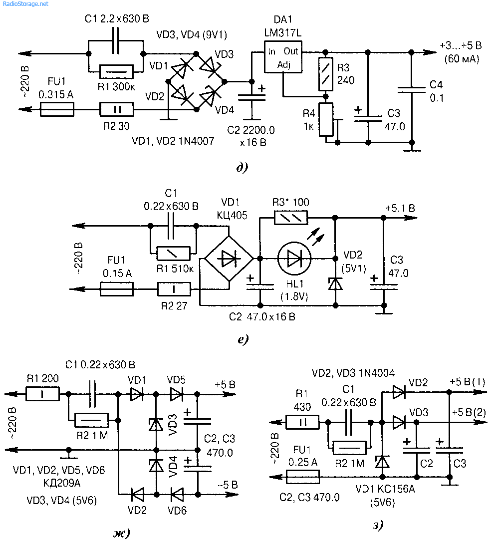
Rice. 6.3. Transformerless power supply circuits with ballast elements (continued):
e) Zener diodes VD3, VD4 have increased power dissipation of 1...3 W and perform preliminary voltage limitation. The stabilizer on the DA I chip provides the output voltage;
f) full-wave rectifier with diode bridge VD1 and LED indication of power availability. Resistor R3 determines the current in the load, as well as the brightness of the HLI indicator. The output voltage depends on the parameters of the zener diode VD2 and the load current;
g) bipolar power supply. For complete symmetry of the circuit, it is desirable to provide equal current loads along the +5 and -5 V circuits;
h) dividing the output voltage into two separate branches to eliminate mutual interference, for example, for powering the MK and for controlling the thyristor. Zener diode VD1 limits the voltage at +5.6 V. Diodes VD2, VD3 reduce it to +4.8...+5 V in each channel;
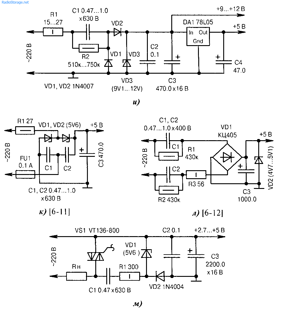
Rice. 6.3. Transformerless power supply circuits with ballast elements (end):
i) receiving two voltages from one power source. The total load current consists of the sum of the currents in the channels +9...+12 V and +5 V. If there are significant fluctuations in the load current, you should choose a VD3 zener diode with increased power dissipation of 1...3 W;
j) Zener diodes VDI, VD2 simultaneously serve as stabilizers and rectifiers. Zener diodes should be chosen that are powerful, with a current reserve;
l) instead of one, two ballast capacitors C1, C2 are used, which can be designed for a lower permissible voltage;
l) in the closed state of thyristor VS1, the current to the transformerless voltage stabilizer (C1...CJ, RL..R3, VDI, VD2) passes through the load RH. Due to the low current value, the load does not operate at full capacity, for example, the lamp does not light, the fan does not spin, etc. After turning on the VSI thyristor, full power is supplied to the RH load, and the voltage at the stabilizer output decreases from +5 to +2.7 V. For the MK to function normally, it must have a wide-range power supply and be able to organize a restart.


Rice. 6.4. Schemes of network transformerless power supply units with AC/DC converters:
a) a typical circuit for connecting a pulsed AC/DC voltage converter on a DA1 microcircuit from ROHM;
b) a typical circuit for connecting a pulse AC/DC voltage converter on the DA1 microcircuit from Power Integrations. Chokes LI, L2 reduce the level of pulsation;
c) a driver for two supply voltages popular among radio amateurs: +5 and +3.3 V. The DA1 microcircuit is a pulse AC1DC voltage converter from Supertex;
t) DAI is a pulse AC1DC voltage converter from Supertex. The total load current across the +18 and +5 V outputs should not exceed 40 mA.
When we are dealing with devices that operate on a low voltage power source, we usually have several options for how to power them. In addition to simple, but expensive and bulky transformers, you can use transformerless power supply.
For example, you can get 5 volts from 220 volts using a quenching resistor or using the reactance of a capacitor. However, this solution is only suitable for devices that have very low current consumption. If we need more current, for example to power an LED circuit, then we will encounter a performance limitation.
If any device consumes a large current and it is fundamentally necessary to power it from a 220 volt network, then there is one original solution. It consists of using only part of the sine wave for power during its rise and fall, i.e. at the moment when the network voltage is equal to or less than the required value.
Description of the operation of a transformerless power supply
The peculiarity of the circuit is to control the opening moment of the MOSFET transistor - VT2 (IRF830). If the current value of the input mains voltage is lower than the stabilization voltage of the zener diode VD5 minus the voltage drop across resistor R3, then transistor VT1 will be closed. Thanks to this, a positive voltage flows through resistor R4 to transistor VT2, as a result of which it is in the open state.
Current flows through transistor VT2 at the moment and the current value of the mains voltage charges capacitor C2. Of course, the voltage in the network drops to zero, so it is necessary to include a VD7 diode in the circuit, which prevents the capacitor from discharging back into the power supply circuit.
When the input network voltage exceeds the threshold, the current passing through the zener diode VD5 causes the transistor VT1 to open. The transistor with its collector bypasses the gate of transistor VT2, as a result VT2 closes. Thus, capacitor C2 is charged only with the required voltage.
Power transistor VT2 opens only at low voltage, so its total power dissipation in the circuit is very small. Of course, the stability of the power supply depends on the control voltage of the zener diode, therefore, for example, if we want to power a circuit with a microcontroller, then the output must be supplemented with a small one.
Resistor R1 protects the circuit and reduces the voltage surge when first turned on. Zener diode VD6 limits the maximum voltage on the control electrode of transistor VT2 to around 15 volts. Naturally, when switching transistor VT2, electromagnetic interference occurs. To avoid transmitting noise to the power grid, a simple LC filter consisting of L1 and C1 components is used in the input circuit.